My first computer build: Part 1 - Introduction, CPU and motherboard
Motivation
I have never built a computer before.
For one reason or another, the timing was never right. Admittedly, the timing still is not right, and as I am writing this, the world is going through some very hard times if you are into enthusiast PC building. The world is in fact going through some hard times in many more aspects right now, but that is beside the point of this write-up. The current chip shortage, along with the disruption to the global delivery chain, combined with an ever rising inflation, has caused the prices of a lot of computer components (especially graphics cards) to skyrocket as of late (that is when they are not simply out of stock). However, having waited for so long, I decided I could not wait any longer and would still try my best at building the system I had dreamed of for so long.
 Figure 1: Lenovo’s Thinkcentre M91p
The closest I had previously gotten to building a computer, was four years ago when I had upgraded a used Lenovo ThinkCentre M91p unit (see Figure 1) I had gotten off Ebay for cheap into a moderately performing gaming PC. This had involved fitting the unit with a mid-range GPU a GTX 1050 Ti (Low-profile because of the ThinkCentre’s small form factor), upgrading the RAM using a 4x 4GB DDR3 kit, and changing the power supply to a 300W unit, in order to supply the graphics card with enough power. Back then, it was the video linked below which really motivated me to try myself at upgrading an old system instead of waiting until I had the money to afford to build a brand new one. I had so much success with that experiment, that I ended up doing it again two more times, building great bang-for-your-buck systems for family members.
I find myself now in a situation where I need a system with more flexibility, higher performance, and different possible future upgrade paths. For these reasons I have decided to finally build myself a computer.
Intended usage of the system
The first step for me was to settle on the use-cases I intended for my future machine. These use-cases would allow me build up a list of requirements I needed my future system to fulfill. My intended uses were:
- Development and compilation jobs:
I want a high core count CPU for heavy compilation loads. In particular, part of the reason why I put my Android Build Guide on hold was because I was using a Linode instance for compiling my lineageOS image. In addition to the instance being limited to 4 cores and 16 GB of RAM, it incurred a monthly cost. Although I was aware of the cost when I first started working on the project, I wasn’t expecting the endeavor to last as long as it did, and the accumulated cost of my Linode instance quickly piled up.
Another reason I want a high core count processor is because I would like to get more into virtualization.
- Light 3D modeling and occasional gaming on Linux:
This requirement pertains mainly to the GPU. I would like to be able to do some casual gaming on Linux. It seems to me that the eco-system has made big strides since I last tried to play something under Linux, and I have been hearing a lot about Proton and Lutris and how they have made the whole experience much more seamless.. I would like to test that for myself.
Additionally, I would also like to get into 3D printing, and therefore modeling.
- Gaming on Windows using PCI pass-through:
This is probably the requirement which pushed me most to build my own system, instead of getting a prebuilt one. As I have mentioned in my previous point, gaming on Linux has made big progress in the last few years. However, some details still need to be ironed out. Particularly, from what I understand, some of the anti-cheat engines used in some online games tend to alright block any online play when an environment that is not Windows is detected. Because of this, it seems like for the time being, running Windows is still a necessity for a seamless gaming experience. This translates into the need for a Linux/Windows dual-boot setup, and the inconvenience of always needing a reboot in order to switch between gaming and productivity.
However, for the last 8 years, PCI pass-through has been gaining a lot of popularity online, as an alternative to this compromise. This alternative relies on using a Windows virtual machine, to which a dedicated graphics card is passed through the PCIe connection, thus achieving near-native performance. This really is the best of both worlds, as one can benefit from the windows eco-system for a seamless gaming experience, without having to trust it with access to the bare-bones of the system’s hardware. The only disadvantage is of course that one needs a capable system, i.e. a system with at least two PCIe slots, and two graphics cards.
What I will be covering in this guide
Because I had never built a complete system from parts before, I had to do a lot of research and learn a lot of things. In particular, I had to catch up on some of the advances PC components and peripherals had made in the last decade (The ThinkCentre M91p was released in 2013 and used an Intel Core i5-2400 which was first released in 2011). In the following I would like to document the things I have found to be the most relevant in my learning, and which I believe are important to be aware of for anyone who is about to take on the same journey that I did.
The Processor
With the intended use-cases of my build defined, I decided to start my quest at the heart of the system: the CPU.
Zen? Ryzen?
In the last five years, AMD has made a monumental comeback with its new Zen architecture, and Ryzen series of desktop processor.
I must have heard this sentence in one form or another dozens of times. I knew from the cyclical coverage of AMD’s releases through the last few years that their Ryzen series of processors was the way to go. However I didn’t know where exactly to start from. The first step for me was to make sense of the previous quote. So let us get started by defining some of its terminology.
 Figure 2: Zen logo
- Zen: is the new processor micro-architecture introduced by AMD back in 20171. A CPU micro-architecture describes the way the instruction-set (machine code at its most basic level) is implemented on the silicon of the processor. The 2017 release used a 14nm process, and marked the first Generation of the Zen micro-architecture. This generation was iterated upon in 2018 with the release of Zen+ on an enhanced 14nm and 12nm processes. Zen2, which marked the third generation was released in 2019 on a 7nm process, and the fourth Generation was released in 2020 under the name Zen3, using a more matured 7nm process. Finally, during the writing of this article, AMD has announced that it will be soon revealing a new generation of CPUs based on its upcoming Zen4 generation.2.
 Figure 3: Ryzen logo
- Ryzen: is the name of the desktop processors which implement the new Zen micro-architecture. Each generation of the Zen micro-architecture was launched with a new family of Ryzen processors, and as I will shortly explain, there is a lot of diversity in the Ryzen series of processors.
- Threadripper: is a line of AMD Ryzen processors more aimed toward the enthusiast workstation market3. This line of processors boasts a higher number of cores, a higher power draw, and perhaps more importantly, a completely different socket.
- CPU Socket: defines the physical slot through which the processor connects to the motherboard. One huge advantage of the Ryzen series of CPUs is AMD’s commitment to support the same socket (AM4) for the first four Generations of the Zen micro-architecture. This has given numerous users to upgrade their processors with each announcement of a new Zen generation without having to throw away their motherboards each time.
Table 1 summarizes what I have just explained about the Zen micro-architecture timeline.
| Generation | Name | Year | Process | Launch processor |
|---|---|---|---|---|
| Gen 1 | Zen | 2017 | 14nm | Ryzen1000 |
| Gen 2 | Zen+ | 2018 | Enhanced 14nm/12nm | Ryzen2000, Threadripper2000 |
| Gen 3 | Zen2 | 2019 | 7nm | Ryzen3000 |
| Gen 4 | Zen3 | 2020 | More matured 7nm | Ryzen5000 |
As I have mentioned earlier, the Ryzen series includes a wide variety of processors. This variety is reflected in the naming scheme of ryzen processors, which is shown in Figure 4.
 Figure 4: Ryzen processors naming scheme
Some of the fields described in Figure 4 require some clarifications:
| Model | Segment |
|---|---|
| Ryzen 3 | Entry-level |
| Ryzen 5 | Mainstream |
| Ryzen 7 | Performance |
| Ryzen 9 | Enthusiast |
| Threadripper | High-End Desktop (HEDT) |
| Threadripper Pro | Workstation |
Segment: This refers to the segment the processor belongs to, different segments have different core counts, frequency ranges, and all around performance. Table 2 shows the meaning of the segment portion of the processor name.
Generation: This reflects the generation of the Zen micro-architecture upon which the processor is built. Table 1 shows the prefix used for each generation.
Power suffix: Perhaps the most important aspect to notice here is that not all Ryzen processors come with integrated graphics, i.e. for such processors a discrete graphics card is a necessity.
Processor layout
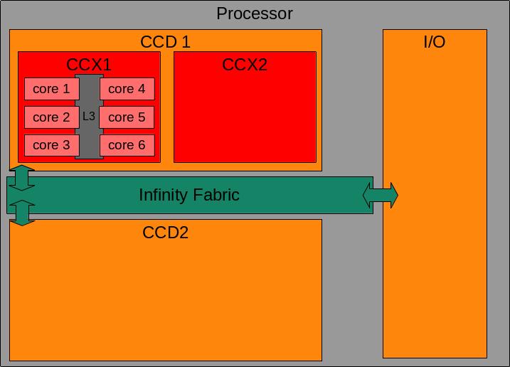 Figure 5: Example layout of a Zen based processor with two CCDs,
each containing two CCXs, themselves housing six cores each
There is one more piece of information I learned along the way, weeding through the different processor models. This relates to the way the cores within a processor are organized in the silicon die.
A simplified block diagram of the layout of a Zen-based CPU is represented in Figure 5. The processor is composed of multiple dies. Some of the dies handle the input/output operations and are simply referred to as I/O Dies. Other dies host the physical cores, these are referred to as CCDs, which stands for Core Complex Dies. Within the CCDs, the cores are organized into groups known as CCXs, or Core Complexes. Cores in the same CCX share L3 cache. Finally, the Infinity Fabric is a high speed communication bus, used to link the different dies.
To crystallize the importance of correctly distinguishing the difference between these different terms, let us compare the Ryzen 7 3800X and the Ryzen 7 5800X. Both these processors have the same core count: 8. However, these cores are organized differently in the two processors. In the case of the Ryzen 7 3800X, these cores are grouped into two complexes (grouped into one complex die), each complex housing four cores. Whereas, in the case of the 5800X, all the cores are organized into one complex containing all eight cores. Figure 6 illustrates this, the figure compares two processors with eight cores each, one being from Zen2 (left) and the other from Zen3 (right), as such the two block diagrams apply exactly to the Ryzen 7 3800X and the Ryzen 7 5800X respectively.
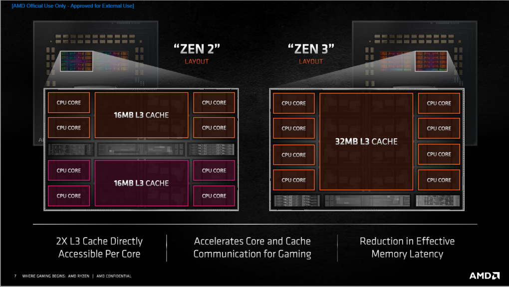 Figure 6: Comparison of Zen2 and Zen3 cores layout
At a first glance, with both processors having the same core count, and the same L3 cache (32MB), one might expect the two processors to have similar performance. However, in the case of the 3800X each CCX has access to 16MB (32MB / 2 CCXs), this cache is shared between 4 cores. In the case of the 5800X, the sole CCX has access to all 32MB of cache, this amount is shared between 8 cores . This means that under multi-threaded loads, requiring multiple cores to exchange data, the 5800X is expected to perform better. This is because the eight cores would have all the data they might need to exchange readily available in the same pool, where as in the case of the 3800X, there is a chance that some data might need to be transferred from the L3 cache of CCX1 to that of CCX2 (or vice-versa), thus incurring extra latency. This difference in core layout on the silicon die is one of the improvements that Zen3 brought over Zen2. Again, this is illustrated in Figure 6.
Final candidates
With the previous information at hand, I now knew that what I needed was at least a Ryzen 7/9 5XXX processor, i.e.a fourth generation model, from either the performance or enthusiast segments. I did shortly consider going the Threadripper route. However, because the Threadripper line of processors uses a different socket (TR4) than the more common Ryzen AM4 socket, I figured it would limit the pool of motherboards I could chose from later. Additionally, the socket would limit my upgradability path to Threadripper only processors. Finally, the price jump when going from Ryzen to Threadripper processors brushed away any regrets I might have had desisting from committing to a Threadripper build.
My search led me to consider the following three models as final candidates for my build:
| Details | Ryzen 7 5800X | Ryzen 9 5900X | Ryzen 3 3900X |
|---|---|---|---|
| Chiplets | 1 × CCD, 1 x I/O | 2 × CCD, 1 x I/O | 2 × CCD, 1 x I/O |
| Core (Threads) | 8 (16) | 12 (24) | 12 (24) |
| Core config: (CCX * cores per CCX) | 1 x 8 | 2 x 6 | 4 x 3 |
| Clock rate: Base (Boost) | 3.8 (4.7) GHz | 3.7 (4.8) GHz | 3.8 (4.6) GHz |
| Cache | L1: 32KB L2: 512KB L3: 32MB | L1: 32KB L2: 512KB L3: 32MB | L1: 32KB L2: 512KB L3: 64MB |
| Socket | AM4 | AM4 | AM4 |
| PCIe lanes | 24 | 24 | 24 |
| Memory support | DDR4-3200 Dual channel | DDR4-3200 Dual channel | DDR4-3200 Dual channel |
| Thermal Design Power | 105W | 105W | 105W |
| Price (When last verified) | 369€ | 489€ | 439€ |
In the Details column, I tried to gather the aspects that defined my choice for these three finalists. I have covered the first three rows (the chiplet, core count, and core configs) in the previous discussion. I don’t have much to say about the cache and socket rows. Finally, We will have a more detailed discussion about the PCIe lanes, memory support, and thermals of the processors in the sections relevant to the motherboard, RAM, and CPU cooler, respectively.
The Ryzen 7 5800X was a strong contender, especially considering its reasonable pricing. However, I was not impressed with the core count, especially when considering my future virtualization and PCIe pass-through ambitions. This made me look into the model above, which was the Ryzen 9 5900X which definitely has enough cores for my intended needs. The only processor above would be the Ryzen 9 5950X which has 16 cores for a total of 32 threads. That would definitely have been very nice to have, however, the increment in core count, comes with close to a 300€ price jump. The Ryzen 9 5900X itself comes with a 100€ price bump compared to the Ryzen 7 5800X. This is why I briefly looked into the Ryzen 3 3900X even though it was one generation older than what I had set for myself. Although the 3900X did have the number of cores I was aiming for, its price was just 50€ shy of that of the 5900X, and it didn’t sit right with me to cheap out on the latest generation just for that price difference. For that reason, the CPU I decided to go with for my build is the: Ryzen 9 5900X.
As reminder, the X in the model name of the processor means that it does not have integrated graphics, and as such, I will need a a discrete GPU for my system.
The Motherboard
Having made the decision in the previous section to go with a Ryzen 5000 processor for my build, a big part of the motherboard question was already automatically solved for me. To explain why this is, I need to define what the chipset in a motherboard is. Historically, the term chipset used to refer to a pair of chips that were present on a computer motherboard in order to handle I/O operations for the processor. These two chips are the North Bridge and the South bridge.
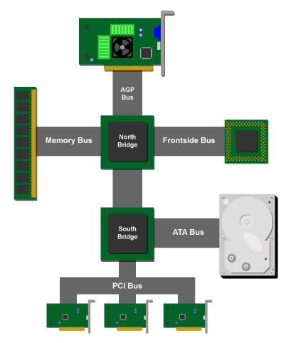 Figure 7: CPU/North bridge/South bridge inter-connection
The North Bridge used to handle connections from the CPU to high speed I/O, particularly the memory and graphical controllers, whereas the South bridge handled low speed peripherals (basically everything else), see Figure 74. However, as CPU performance increased, the North bridge started becoming a bottleneck for communication between the CPU and high speed devices, and ended up being integrated into the CPU. Now the term Chipset, refers to the chip which handles tasks historically delegated to the South Bridge, i.e. read and write operations to storage disks, and some USB and PCIe devices. Because the chipset works in such close proximity (logically, not necessarily physically) to the processor, different families of processors require different families of chipsets. In fact different generations of the same family of processors would not have inter-compatible chipsets.
Figure 85 showcases the different generations of AM4 compatible chipsets, and the Ryzen generations they support. When first announced in 2019, the X570 and B550 chipsets were the only ones revealed to have future support for the Zen3 architecture (i.e. Ryzen 5000 processors). Later in February 2021 AMD announced6 it would extend Support for the Ryzen 5000 processors to X470 and B450 motherboards through Manufacturer-issued BIOS update. Finally, support for the much older Ryzen 1000 and 2000 CPUs seems to be made available by some manufacturers through BIOS updates 7.
This is what I meant earlier, when I said that part of the motherboard question was already answered for me. I will have more to say about the BIOS update process later in this section, but for now, suffice it to say I did not want to have to deal with it on top of everything else. As such, my choice was already “restricted” to either a X570 or a B550 motherboard.
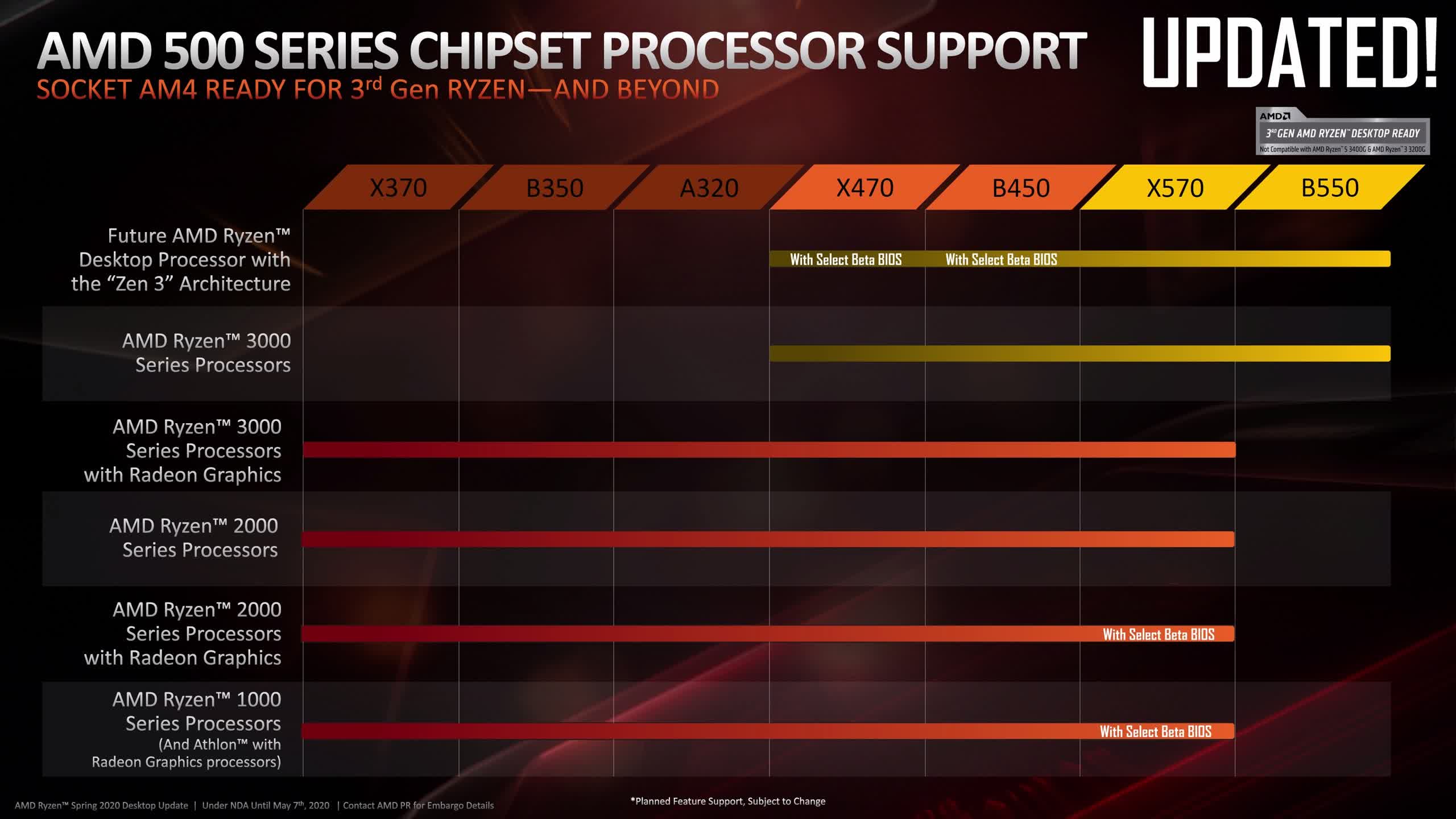 Figure 8: AMD AM4 chipsets support
The X570 chipset was launched in July 2019 and belongs to AMD’s high-end X-series chipsets. Motherboards of this series support the largest feature set, including AMD’s crossfire/Nvidia’s SLI (i.e. the ability to use multiple graphics card in tandem) and overclocking. The B550 was launched almost a year later in June 2020 and is part of the more mid-range B-series chipsets. The B-series supports less features than the X-series, this is most reflected in a lesser count of PCIe slots. There exists one more series of AMD chipsets, the A-series, which is the most budget of the three, with only the minimal features being supported.
The main difference between the X570 chipset and B550 is in the type of supported PCIe lanes. In order to fully understand this difference we need to take the following short detour.
The PCIe interlude
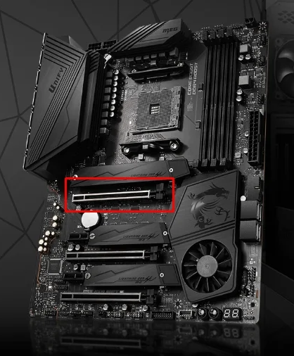 Figure 9: PCIe slot on the MSI X570 MEG Unify motherboard
PCIe, stands for Peripheral Component Interconnect Express. It is a high-speed computer communication expansion bus, which came as the successor to the older PCI bus. PCIe is usually read simply “PCI Express”. PCIe expansion cards can be connected to the onboard PCIe bus through PCIe slots. Figure 98 highlights what these slots look like. The speed of a PCIe connection depends on two factors:
The Number of communicating lanes: A PCIe connection is composed from 1 up to 16 lanes (similar as to how a highway is made up from multiple lanes).. Each lane is made up of two separate differential signaling pairs, making it a full duplex channel, i.e. Transmit and Receive operations are independent and can happen simultaneously. PCIe channels are defined by their width. This width represents the number of lines making up the channel, and has usually one of the following values: 1, 4, 8 or 16. The overall bandwidth of PCIe connection equals the number of lanes in the connection times the base bandwidth of a single lane.
The PCIe generation: The base bandwidth of one PCIe lane depends on the PCIe generation. Table 49 shows the evolution of PCIe speed throughput through its different generations. Traversing Table 4 from left to right, reveals that when first introduced in 2003, one PCIe Gen 1.0 lane had a throughput of 250MB/s. This throughput was doubled with every generation, reaching a maximum of almost 8GB/s for the upcoming sixth generation, which was announced during the writing of this article10. Observing Table 4 from top to bottom, the throughput is multiplied by the number of lanes in the channel. Do note that as of the writing of this article, PCIe Gen 6 is not yet supported by any processor in the market, and that only Intel’s latest 12th Generation CPUs support PCIe Gen 5. Additionally, AMD’s next generation Ryzen 7000 series processors have also been revealed to having support for PCIe Gen 52
| Total lanes | PCI Express Bandwidth (GB/s) | |||||
| PCIe 1.0 (2003) | PCIe 2.0 (2007) | PCIe 3.0 (2010) | PCIe 4.0 (2017) | PCIe 5.0 (2019) | PCIe 6.0 (2022) | |
| x1 | 0.25GB/sec | 0.5GB/sec | ~1GB/sec | ~2GB/sec | ~4GB/sec | 8GB/sec |
| x4 | 1GB/sec | 2GB/sec | ~4GB/sec | ~8GB/sec | ~16GB/sec | 32GB/sec |
| x8 | 2GB/sec | 4GB/sec | ~8GB/sec | ~16GB/sec | ~32GB/sec | 64GB/sec |
| x16 | 4GB/sec | 8GB/sec | ~16GB/sec | ~32GB/sec | ~64GB/sec | 128GB/sec |
- Mechanical vs. electrical width: This is a very important point to understand. The PCIe slots, to which PCIe devices connect, have a mechanical width which is reflected in the physical width of the slot. However, it is possible that the the physical ports which make up a PCIe slot are not all populated with electrical pins, and thus, not connected to PCIe lanes. This is shown in Figure 108. Both PCIe slots shown in Figure 10 have a x16 mechanical width (they have the same physical width). However, whereas the top slot has all of its physical ports populated with electrical connections, the bottom slot only has the left half of its mechanical width being populated by electrical pins. If you zoom in, you can almost see the copper pins at the immediate left side of the blue/red rectangle separation. What this amounts to, is that even though a motherboard might have a PCIe x16 slot, you will still have to check how much of the slot is actually wired to know its real bandwidth. You can always plug a PCIe expansion card into a PCIe slot even if they are not of the same physical size (e.g. a x1, x4, x8 card can always be mounted on a x16 slot), as the available lane count is negotiated with the PCIe host during initialization. However, the bandwidth will be limited by the number of (electrical) lanes available to the slot.
Motherboard manufacturers describe a PCIe slot using the following notation: PCIe xa (xb) where a is the mechanical width, and b is the electrical width. Following this notation, the two PCIe slots present in Figure 10 are x16 (x16) in the top half and a x16 (x8) in the bottom half.
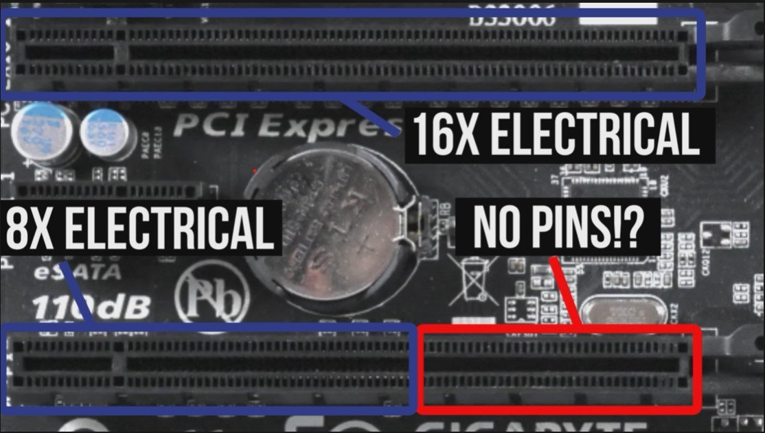 Figure 10: Top: x16 (x16) PCIe slot, Bottom: x16 (x8) PCIe slot
Following the previous discussion, I was able to calculate the bandwidth of any PCIe slot, knowing the generation used on the motherboard, and the total width of the PCIe channel. The next question to answer for me was:
How much PCIe bandwidth do I actually need?
The required bandwidth depends on the actual device being connected to the PCIe slot. There exists a multitude of PCIe expansion slots. These can be USB/Network Adapter cards, Flash storage devices, capture cards, etc. I cannot cover every possible PCIe device. However, I will cover what is arguably the most common one, that being, a GPU.
Although GPU manufacturers readily advertise the specification of the Bus interface their cards are using, that information only gives defines the theoretical maximum bandwidth of the card’s interface. I did try to find online resources about the actual used bandwidth of these devices under normal loads, but couldn’t find any concrete values to showcase here. I did however find some resources that gave me a good idea of the bandwidth requirements of a modern GPU. Table 58 showcases the Bus interface of some Nvidia GPUs from the last three generations, as well as the measured minimum generation and number of PCIe lanes required to avoid PCIe bottleneck. What this table shows, is that the Bus interfaces of these GPUs are largely over-sized for their actual bandwidth usage (at least under gaming load). In fact, for most of these GPUs, one can use systems with half the required bandwidth and get away with less than 1% performance loss. Additionally, The extensive testing done by GamersNexus11 has shown that using PCIe 3.0, under gaming scenarios with either a 1440p or 4K resolution, downgrading the GPU connection from a PCIe x16 to a PCIe x8 slot (i.e. effectively halving the maximum bandwidth) resulted in inconsequential differences in FPS performance which were within the margin of error.
| GPU | Bus interface | Required PCIe Gen. & Lane Count for < 1% performance loss | Required PCIe Gen. & Lane Count for < 5% performance loss |
|---|---|---|---|
| GTX 1660 Super | PCIe 3.0 x16 | PCIe 3.0 x4 | PCIe 3.0 x4 |
| RTX 2060 Super | PCIe 3.0 x16 | PCIe 3.0 x8 | PCIe 3.0 x4 |
| RTX 2080 Ti | PCIe 3.0 x16 | PCIe 3.0 x16 | PCIe 3.0 x8 |
| RTX 3060 Ti | PCIe 4.0 x16 | PCIe 4.0 x8 | PCIe 4.0 x4 |
| RTX 3080 | PCIe 4.0 x16 | PCIe 4.0 x8 | PCIe 4.0 x4 |
| RTX 3090 | PCIe 4.0 x16 | PCIe 4.0 x16 | PCIe 4.0 x8 |
X570 vs. B550
What pushed us towards the previous tangent, was the fact that the main difference between X570 and B550 chipsets resides in the PCIe support. In fact, for B550 the link between the CPU and the chipset is a PCIe 3.0 x4 channel, whereas the X570 chipset uses a PCIe 4.0 x4 channel. With the discussion of the previous section, we now know that this means that X570 allows double the bandwidth between the CPU and the chipset compared B550. This is important considering that a lot of peripherals (SATA disks, USB I/O, some NVMe ports) will be all connected to the CPU through the chipset, and as such will have to share this channel. This aspect is doubly important for my future PCIe pass-through setup, as I will need to use at least two PCIe slots, and if one of them is wired through the chipset, then it will have to share the CPU-chipset channel with whatever other devices I might have connected to my motherboard through the chipset, thus incurring possible bottleneck. With that being said, Table 5 has shown that any modern GPU would probably not complain about the limited PCIe bandwidth on a B550 motherboard. However, considering I didn’t know how much peripherals I might end up connecting to the motherboard, I opted to air on the side of caution and go with an X570 motherboard. Other advantages of X570 over B550 which encouraged my in my choice included the support of more USB 3.2 Gen 2 ports (maximum of 8 vs. 2 for B550), with USB 3.2 Gen 2 boasting a throughput of 10Gbps compared to Gen 1’s 5Gbps, and a higher count of PCIe and NVMe slots12. Figure 11 shows a block diagram of the supported I/O on the X570 chipset.
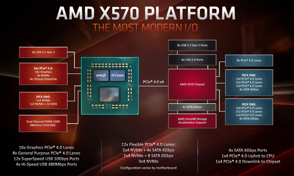 Figure 11: Block diagram of X570 I/O
Additional parameters to consider in a motherboard
In addition to the socket and chipset used by the motherboard, there were other details I considered when weeding through the different motherboard models. The following is a listing of these details in the order of their importance to me:
- PCIe and NVMe slots count: As I have explained earlier, considering my future PCIe pass-through plans, I needed a motherboard with at least two PCIe slots. Additionally, I set two NVMe slots to also be a minimum for me.
- BIOS quality and upgradability: I needed the firmware of the motherboard to be one with positively reviewed online, and where important settings weren’t hidden behind a maze of menus. As we saw in the previous section, X570 motherboards do support Ryzen 5000 processors. However, depending on when they were produced, different motherboards of the same manufacturer and of the same model might come with out-of-the box support for Ryzen 5000, or might require a BIOS update for that. This could lead to a chicken and egg problem, wherein, in order to use a Ryzen 5000 processor on one of these boards, a BIOS update is required. However, in order to be able to update the BIOS, a CPU is needed to boot the motherboard… If you are upgrading your motherboard and already have an older Ryzen CPU, then this is not a problem. However, this was not the case for me.
Thankfully, a CPU is not always needed in order to update the BIOS on a motherboard. Some motherboards include of a BIOS flash button, and support flashing a binary BIOS file directly from a USB stick when this button is pressed. In this case, no CPU nor RAM are needed, the motherboard only needs to be plugged into a power supply. This Feature is sometimes referred to as BIOS Flashback13 or Q-Flash14 depending on the motherboard manufacturer, so be on the lookout for similar terms if this feature is of interest to you. - Good IOMMU support: This relates to my intended PCIe pass-through future use-cases. Without getting into details (because frankly, at this point in time those remain unclear to me too), the firmware of a motherboard groups its different ports into different groupings called IOMMU groups. What this means, is that if I wanted to pass a secondary GPU to a virtual machine, while keeping my main GPU under the host system, the two PCIe slots onto which the two GPUs would be mounted, needed to be in two separate IOMMU groups. Otherwise it would be simply impossible to separate them that way. The IOMMU groups of a motherboard depend on both the hardware and the firmware it is using, so they can change following BIOS updates. The way I checked this parameter, was by looking online for people who managed to get PCIe pass-through to work on the specific motherboard I was looking into. I am planning on having a separate article where I will discuss the topic more in details, so be on the lookout for it.
- VRM performance: VRM stands for Voltage Regulator Module. These components handle converting the voltage from the motherboard’s 12V to the lower voltages required by the CPU and the chipset (less 1V). Stable VRMs ensure a stable operation of the processor. Additionally, these components end up generating a lot of heat due to the current they end up conducting, and higher-end motherboards usually have large heat sinks to keep the VRM temperatures within a reasonable range.
- Chipset Fan noise level: As we have covered, X570 motherboards support a PCIe 4.0 link between the CPU and the chipset. This increased bandwidth comes at a price of increased heat generation at the chipset. For this reason, X570 motherboards include a fan on top of the chipset. This fan introduces a new possible source of noise, which needs to be taken into consideration if the noise level of the system is an important aspect.
- On-board diagnosis: This includes diagnostics LEDs, and seven-segment displays. Such indicators can make life much easier if some tinkering on the motherboard is planned, e.g. BIOS updates, overclocking.
- USB headers count and type: Pretty self explanatory, the more USB headers on the motherboard the more USB ports the system can have. Latest generation USB 3.1 Gen 2 and USB Type C headers were on my must-have list.
- On-board temperature sensors and Fan/Pump PWM headers: Having these two features and combining them allows to configure costume fan profiles which can be optimized for either performance or noise level.
- Back plate I/O: The more connectivity the better.
- Integrated Wi-Fi/Bluetooth: Always a plus, for network redundancy and Bluetooth audio.
- Overclocking support: I am not planning on any future overclocking. However, motherboards advertised by their manufacturers as “Overclock ready” or “optimized” usually have more thought put into the BIOS and come with better quality VRMs.
- RGB lighting and control: I am not a fan of RGB lighting on a motherboard. However, I am okay with RGB lighting if it can be controlled from the BIOS. Requiring a specific software to configure/disable RGB lighting is a very strong “no” for me. Such software constitutes bloatware, and usually is shipped only as Windows binaries, with Linux support being left as a reverse-engineering exercise for anyone interested.
- RGB headers: As I said in the previous point, I am okay with RGB as long as I can control it. RGB headers are a plus for me as they give me the option to use RGB headers or strips if I ever decide I want to try them.
With the previous list, I believe I have covered all aspects that I took into consideration when making my way through the seemingly unending list of motherboard models out there.
Final candidates
In the following section I will highlight the two motherboards which made to it as final candidates to my build.
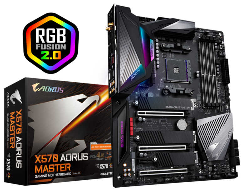 Figure 12: GIGABYTE X570 AORUS Master
- GIGABYTE X570 AORUS Master
- Useful reviews: [1], [2].
- Pros: From my research this motherboard seemed to have a sizable online community when it comes to PCIe pass-through. From what I could find online its VRMs are on the very high-end side, and come with very large heat-sinks. The board has three x16 PCIe slots (x16, x8, and x4), and three NVMe slots. The I/O is phenomenal, even having two Ethernet ports: a 2.5Gbps and a 10Gbps(!!). Additionally, lots of fan headers and thermal sensors are available, and the onboard diagnosis is all what one can ask for. All around, this motherboard seems to be one of the best X570 boards out there.
- Cons: Too much RGB for my taste, and no way to control it in the BIOS. Looking through online reviews, I found that a lot of people have had a lot of issues with the first revision. Particularly, relating to overheating. It seems Gigabyte has fixed these issues in subsequent revisions (so far the board is at revision 1.2 following rev 1.1 and the initial rev 1.0). However, as of end of 2021, when ordering one of these motherboards it seemed to be a total toss-up as to which revision would be delivered, as it was entirely dependent on the seller’s stock. Finally, the audio chip used on the motherboard has some driver issues under Linux, and during my research it seemed to me that these issues still hadn’t been resolved.
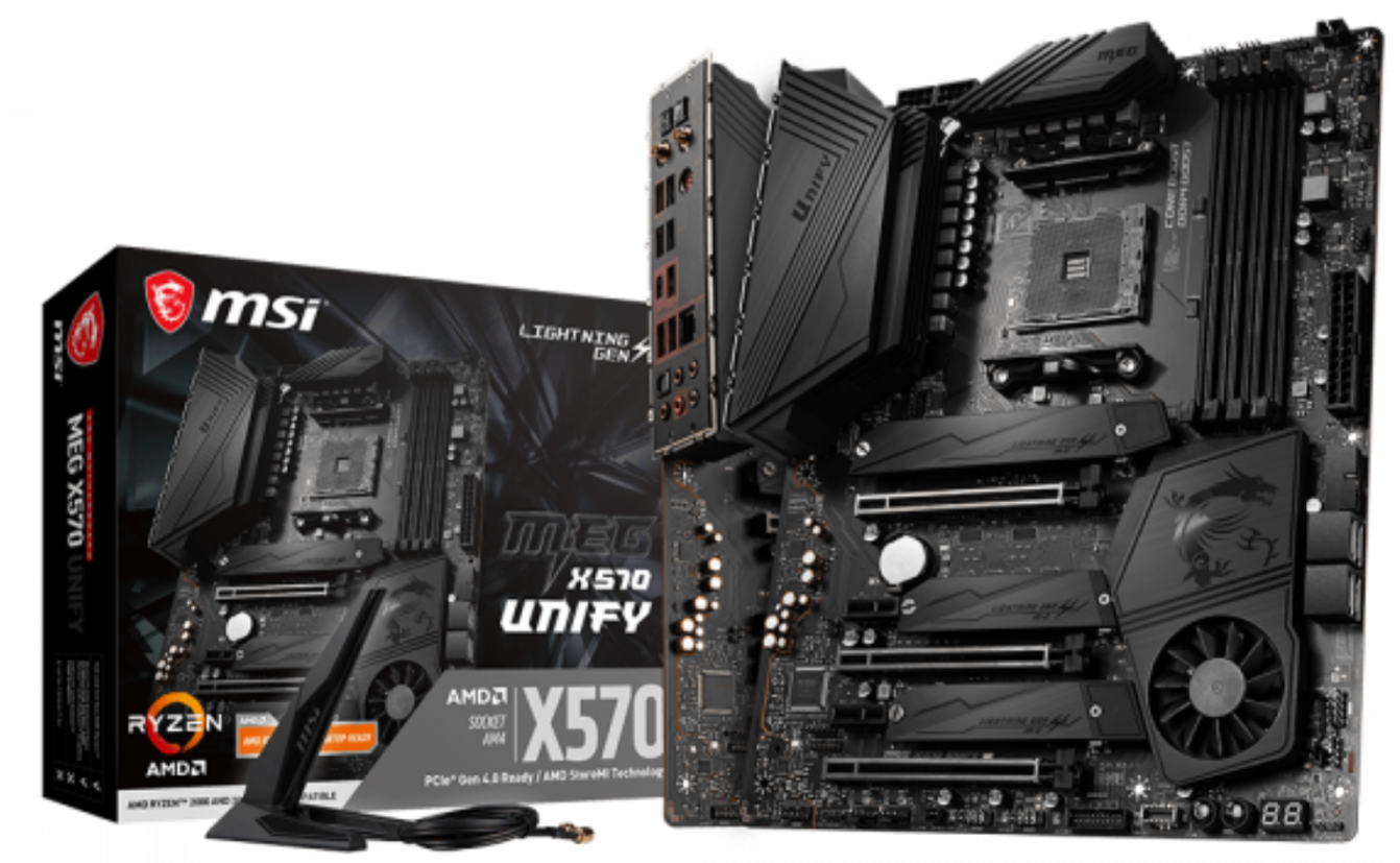 Figure 13: MSI MEG X570 Unify
- MSI MEG X570 Unify
- Useful reviews: [1], [2].
- Pros: Three x16 PCIe slots (x16, x8, and x4), and three NVMe slots. Online reviews of this board are very positive, and I found at least one other person who managed to get PCIe pass-through to work on it. Additionally, the first two PCIe slots are bifurcated. What this means is that if only the first PCIe slot is populated, it is given the full x16 bandwidth. If the second slot is also used, then the x16 bandwidth is halved between the two slots (x8 + x8). The advantage being that both these PCIe slots, are directly connected to the CPU instead of one of them being routed through the chipset. A 2.5 Gbps Ethernet port is present, and the board has integrated Wi-Fi 6 and Bluetooth 5. Finally, the board has a full blackout design with no RGB, which I really like. The board also has four LED headers, one of them being compatible with a Corsair branded RGB hub.
- Cons: The biggest gripe for me with this motherboard is the back-plate connectivity. Particularly, I don’t understand why the designers of the board opted for a PS/2 dual-port instead of fitting two more USB ports in the same space. There is also more unused space on the back-plate which could have housed more USB ports.
One thing about both motherboard, is that neither comes with video output on the back-plate. This is of course not an issue for me as the Ryzen 9 5900X CPU I have settled on in the previous section does not have integrated graphics anyway. Any video output I will have from my system will come from the GPU, which has its own video output ports.
The GIGABYTE X570 AORUS Master truly looks like the perfect board for the job. However, the very real possibility of getting an old revision model in the mail and having to deal with that headache of getting it replace, in combination with the (apparently) as of yet unsolved issue with the audio chip driver made me desist on choosing it. Having no option to control RGB in the BIOS was also a big turn off for me. Finally, perhaps it was a lack of imagination on my side, but I couldn’t think of any use-case where I would need two Ethernet ports (one of them being of 10GB no less!), and it felt like waste getting the board and not fully using it. For these reasons, I decided to go with the MSI MEG X570 Unify. As I have said, I find the back-plate I/O to be a bit disappointing, but my plan is to use USB PCIe expansion cards, or USB header-to-panel adapters in case I really need the extra connectivity.
In the next installment
When I first started writing this article, I envisioned to cover all the information I gathered about all the different computer components in a single article. However, just covering the CPU and motherboard revealed itself to require a lot of work and a longer discussion than I anticipated. This article ended up being longer than I expected, but I didn’t want to split the CPU and motherboard sections considering how coupled these two components are. These two components are also the two that required the most learning on my part, and which required the most research. In the next section I hope to be covering most of the remaining parts, and I believe the discussion will not require getting as much into details as this one did.
Until then!